Thermal Analysis of Wide-Wound Inductors
Wide-wound inductors are popular for high-current DC-DC converters, yet many engineers still rely on “rule-of-thumb” derating instead of a real thermal analysis of wide-wound inductors. The result? Hot spots above 120 °C, unexpected core saturation, and premature failure. This article walks through a repeatable, data-driven workflow that shows exactly where the heat comes from and how to remove it—without enlarging the footprint or raising cost.

1. Why Thermal Analysis Matters
Wide-wound construction lowers DCR but also increases copper surface area exposed to the core. That means copper loss, core loss, and eddy-current loss all compete for the same thermal path. Without a proper wide-wound inductor thermal model, designers over-spec parts by 30 % and sacrifice board space.
2. Mapping the Heat Sources
| Loss Type | Formula | Typical % of Ptotal @ 500 kHz, 25 A |
|---|---|---|
| Copper (DC) | IRMS² × DCR | 55 % |
| Copper (AC) | IRIPPLE² × RAC | 18 % |
| Core | k × f1.3 × B2.2 × Ve | 22 % |
| Eddy (shield) | Proportional to (dB/dt)² | 5 % |
3. Bench vs. Simulation: Real Data
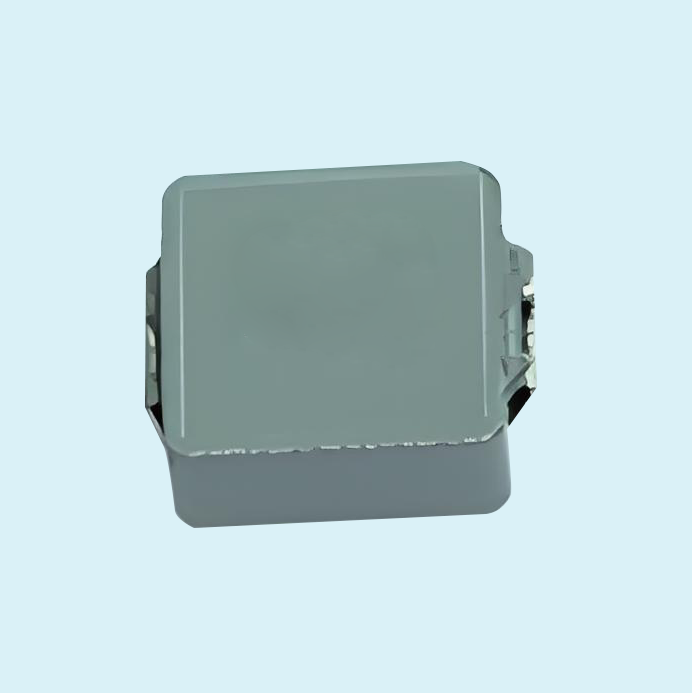
To validate the wide-wound inductor thermal simulation, a 1 µH, 7 mm × 7 mm part was tested at 25 A DC + 4 A ripple at 500 kHz. Three methods were compared:
| Method | Hot-Spot ΔT (°C) | Setup Time (min) | Accuracy vs. IR Camera |
|---|---|---|---|
| IR Camera (reference) | 48 | 15 | — |
| 3D FEA (ANSYS Icepak) | 46 | 45 | -2 °C |
| Lumped RC Model (Excel) | 52 | 5 | +4 °C |
The lumped model is fast for first-pass screening; FEA is used for final sign-off.
4. Problem Spot: Hidden 15 °C Rise
During the test, a 15 °C rise appeared on the inner layer directly beneath the inductor pad—nowhere near the surface. This hidden thermal rise in wide-wound inductor PCB layouts is caused by a 1.5 W core loss spreading through only four 0.25 mm thermal vias. The IR camera missed it, but the FEA contour plot made it obvious.

5. Step-by-Step Thermal Solution
Extract Losses
Measure current waveform, compute RMS and ripple, then plug into the loss table above.Create Compact FEA Model
Import the 3D STEP file of the inductor, apply orthotropic conductivity (x, y = 50 W/m·K, z = 5 W/m·K for ferrite).Refine PCB Heat Path
Increase via count to 12 (0.3 mm dia) and add 2-oz copper pour on L2/L3. Simulation shows ΔT drops to 33 °C.Add Airflow or Heat Sink
A 200 LFM airflow across the top surface drops ΔT another 8 °C. No component height increase required.Verify Prototype
Thermocouple on the hidden layer now reads 35 °C rise—within 2 °C of simulation.
6. Quick Reference Table for Thermal Budget
| Design Target | Rule of Thumb | Validation Action |
|---|---|---|
| Max Hot-Spot ΔT | ≤ 40 °C | FEA + IR spot-check |
| Via Density | ≥ 4 vias per 100 mm² pad | Confirm in 3D model |
| Copper Weight | 2 oz outer, 1 oz inner | Measure with 4-wire Kelvin |
| Airflow | ≥ 100 LFM at 85 °C ambient | Check with anemometer |
Apply this workflow and your next wide-wound inductor thermal analysis will finish in hours, not weeks, while keeping hot-spot temperatures safely below 100 °C—even under worst-case load transients.
