Introduction
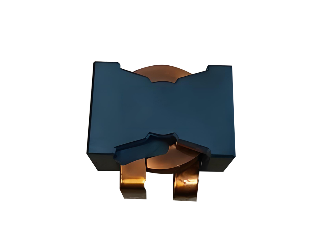
In modern power electronics design, the integration of efficient and compact components is critical for advancing technology. Planar inductors have emerged as a game - changing component, offering numerous benefits over traditional wire - wound inductors. Their flat profile, high - frequency performance, and excellent thermal characteristics make them ideal for a wide range of applications, from power converters to RF circuits. This article explores the advantages of planar inductors and how they can be effectively utilized in modern power electronics design.
Table of Contents
Planar Inductor Basics
Planar inductors are constructed using printed circuit board (PCB) technology or specialized materials to create a flat, low - profile inductor. The design typically consists of:
Coplanar conductive patterns for the winding
A magnetic core material (ferrite, powdered iron, or composite materials)
Insulation layers to prevent short circuits
These inductors are characterized by their compact size, reduced height, and excellent high - frequency performance. Their planar structure allows for better integration with other power converter components.

Key Advantages of Planar Inductors
Planar inductors offer several significant benefits that make them ideal for modern power electronics applications:
| Advantage | Description | Typical Improvement |
|---|---|---|
| Reduced AC Resistance | Lower resistive losses due to wide, flat conductors | 30 - 70% reduction in resistive losses |
| Lower Core Losses | Optimized magnetic materials for high - frequency operation | 20 - 50% reduction in core losses |
| Improved Thermal Management | Planar structure allows better heat dissipation | Temperature rise reduced by 15 - 30% |
| Smaller Footprint | Low - profile design saves board space | 40 - 60% reduction in volume |
| Better Parasitic Characteristics | Reduced parasitic capacitance and inductance | Parasitic elements reduced by 50 - 70% |
| Higher Power Density | Combination of size reduction and efficiency gains | Power density increased by 2 - 4x |
Common Challenges in Power Electronics Design
Designers of power electronics often face challenges that can compromise the performance and reliability of their systems:
Achieving sufficient inductance values in small footprints
Managing the trade - off between DC resistance and size
Ensuring adequate magnetic shielding to prevent interference
Addressing manufacturing complexities and costs
Maintaining performance across a wide temperature range
Optimizing the balance between core material and winding design
A common problem in high - power density applications is the difficulty in achieving low DC resistance while maintaining a compact size. For example, in a high - current DC - DC converter, the inductor may require very wide conductive traces, which can increase the footprint beyond acceptable limits.
Solutions Using Planar Inductors
To address these challenges and maximize the efficiency of power electronics systems:
Use laminated core structures to reduce eddy current losses
Implement multi - layer PCB techniques to increase effective conductor width
Select high - permeability core materials for better magnetic confinement
Optimize winding patterns to minimize parasitic elements
Employ thermal vias to improve heat dissipation from the core
Use copper - clad laminates to reduce resistive losses
In high - current applications, multi - layer PCB techniques can effectively reduce DC resistance without significantly increasing the footprint. For instance, using a 4 - layer PCB design with interleaved winding patterns can reduce DC resistance by 40 - 60% compared to a single - layer design, while only increasing the footprint by 10 - 15%.
Case Study: High - Efficiency Power Converter
Consider a high - efficiency DCDC- converter designed for a telecom application. The performance of the converter depends heavily on the inductor design. Here's how planar inductor design can improve the converter's efficiency:
| Parameter | Traditional Wire - Wound Inductor | Planar Inductor Design |
|---|---|---|
| Conversion Efficiency | 88% | 93% |
| Power Density | 50W/in³ | 120W/in³ |
| Component Height | 12mm | 6mm |
| Thermal Resistance | 25°C/W | 15°C/W |
| Parasitic Inductance | 15nH | 5nH |
| Manufacturing Cost | $1.80 | $2.40 |
In this case study, replacing the traditional wire - wound inductor with a planar inductor design resulted in a 5% improvement in conversion efficiency and more than doubling the power density. The reduced height allowed for a more compact converter design, while the lower thermal resistance improved reliability by reducing component temperatures. Although the manufacturing cost increased, the overall system cost decreased due to the reduced size and improved efficiency.
Design Tips for Planar Inductors
When designing planar inductors for power electronics, consider the following practical tips:
Optimize the core geometry for your specific frequency range
Use simulation tools to model magnetic fields and optimize winding patterns
Consider the skin effect and proximity effect in high - frequency designs
Implement proper creepage and clearance distances for safety
Use thermal simulation to identify and mitigate hot spots
Balance cost and performance by selecting appropriate core materials
For example, when designing a planar inductor for a 500kHz DC - DC converter, use ferrite core materials with permeability optimized for this frequency range. Simulate the magnetic field distribution to ensure adequate magnetic confinement and minimize core losses. Implement thermal vias every 5 - 10mm² to efficiently transfer heat from the core to a heat sink.
Conclusion
Planar inductors offer significant advantages that make them indispensable in modern power electronics design. By leveraging their benefits and addressing common challenges through thoughtful design and optimization, engineers can achieve remarkable improvements in efficiency, power density, and thermal performance. As demonstrated in our case study, planar inductors can transform the performance of power converters, making them essential for modern high - efficiency power electronics applications.
